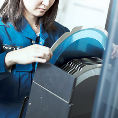
Cutting and Planarization Using a Surface Planer
Solutions
Surface planners use bit grinding with a diamond bit to realize high-accuracy planarization for ductile materials (Au, Cu, and solder), resin (photoresist, polyimide), and composites of these materials.
Advantages of the surface planer
- Achieves high-precision cutting and planarization using a diamond bit
- Because cutting is used, high-quality processing is possible even for composite materials such as resins and metals
- Increases productivity and reduces costs by partially replacing CMP processes
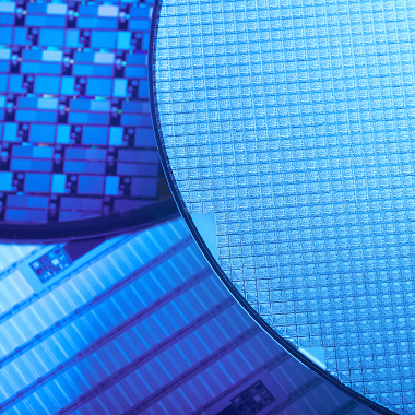
Examples of surface planer processing
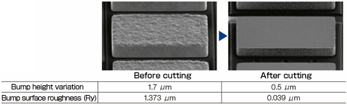
Cutting metal plated bumps(LCD driver IC)
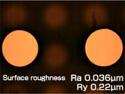
By cutting bumps, the surface planer eliminates bump dents and shoulder overhangs, and solves the issues of bump height variation and surface roughness.This increases the ACF(Anisotropic Conductive Film) effective capture area on the bump surface.
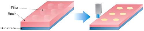
Batch cutting of copper pillars and resin(pillar exposure)
The surface planer cuts resin in which copper pillars are embedded and exposes the pillars.The planarization of the top surfaces of these pillars increases the reliability of connection with other devices.We are also studying a connection method in which the planarization and exposure of solder bumps are performed for each resin piece.
-
Before cutting
-
After cutting
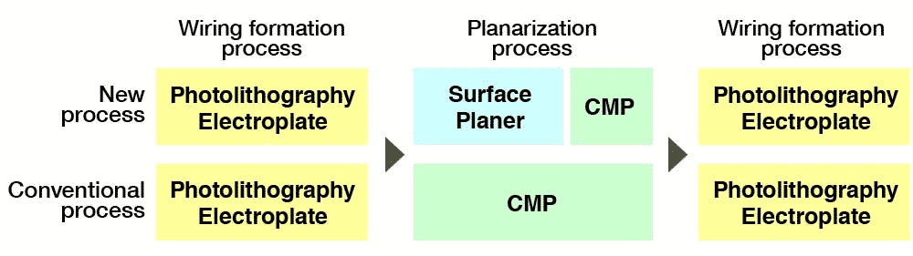
Replacing CMP processes
Usually, CMP is used for planarization when batch planarization is performed for copper wiring formed on
wafers and insulating film, and a wiring layer is then placed on top.Using the surface planer in this process
achieves a throughput that is even better than CMP. Also, because slurry is not used, wastewater
processing costs and environmental burdens are reduced.
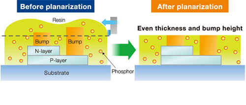
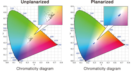
LED phosphor resin planarization
Variations in resin thickness of the LED emission unit is the cause of color irregularities. Planarization of the resin and bumps with high accuracy using a diamond bit can contribute towards the stabilization of LED color emissions.
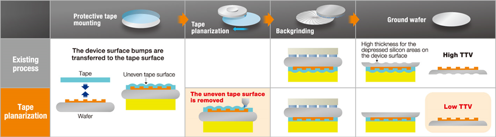
Protective tape planarization
Backgrinding of wafers with large bumps can result in high wafer thickness variation. The final wafer surface thickness variation can be reduced by tape planarization prior to grinding.
Related Information
List of Surface Planers
https://www.disco.co.jp/eg/products/index.html?id=planarization
Contact
Please feel free to contact us with any questions or inquiries.
-
Applications Support
A free-of-charge test cut is performed at an application lab to confirm whether achieving the customer's needs is possible.
Details -
Dicing and Grinding Service
It is effective in sample and prototype manufacturing during development or low-volume production. Designated engineers will provide support based on the desired leadtime and at reasonable cost.
Details