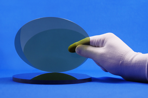
This is an ingot slicing method where a separation layer (KABRA layer) is formed at a specified depth by continuously irradiating an ingot with a laser, producing wafers starting from the KABRA layer.
In addition, this process can be applied to various types of SiC ingots, including single-crystal (4H, 6H, and semi-insulation) and multi-crystal ingots. This process can be also applied to monocrystal ingots, regardless of the off-angle of the crystal c-axis.
In addition, this process can be applied to various types of SiC ingots, including single-crystal (4H, 6H, and semi-insulation) and multi-crystal ingots. This process can be also applied to monocrystal ingots, regardless of the off-angle of the crystal c-axis.
- *1: Patented / Trademark registered


The existing methods for slicing wafers from a SiC ingot mostly used a diamond wire saw. However, these methods require a number of diamond wire saws for mass-producing wafers because the processing time is long due to the high hardness of SiC. The number of wafers produced from a single ingot is also small due to a large amount of material lost in the slicing sections. This has been a major factor in the increased cost of producing SiC power devices.


Processing time is
greatly reduced
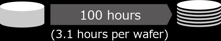
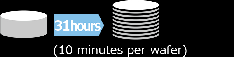
Existing processes require approx. 3.1 hours to slice a wafer from a Φ6-inch SiC ingot (100 hours for one ingot)*2, 3. In contrast, KABRA can greatly reduce the processing time, requiring only 10 minutes to slice a wafer (approx. 31 hours for one ingot)*4.
- *2: When producing a specified thickness of 350 µm from Φ6-inch and 20 mm thick SiC ingot.
- *3: General value based on users' information.
- *4: When laser irradiation, separation, and ingot grinding are performed in parallel using multiple ingots.
Existing process
KABRA process

Lapping process is
no longer required
For wire processing, a lapping process is required to remove approx. 40 µm*3 of undulations generated on the surface of a processed wafer. However, KABRA does not require lapping because the wafer undulation after separation can be controlled.
- *3: General value based on users' information.
Existing process
KABRA process

Number of wafers produced increases
1.4 times more than
that of existing processes
While wire processing produces approx. 180 μm*3 of material loss per wafer where the ingot is sliced (kerf loss), KABRA has essentially no material loss. In addition, material loss can be suppressed to approx. 80 μm depending on the amount of KABRA layer removal after separation. Thus, approx. 1.4 times as many wafers can be produced from a single ingot compared to the existing process.
- *3: General value based on users' information.
Existing process
KABRA process


Fully Automatic KABRA System
KABRA!zen®
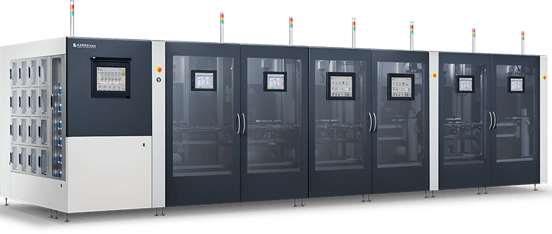

Φ8 inch ingot processing
Supports a maximum ingot thickness of 40 mm
- Machine dimensions (W×D×H):6,740×2,755×1,800 mm

“Kabra” is also another name for a turnip, and thin slicing is sometimes called “kabra-giri”. There is also a vegetable called “kyo-kabra” which is a traditional food with a long history in Japan. We named this process “KABRA” with Roman letters because slicing a SiC ingot looks like “kabra-giri” and we have the strong desire to contribute to enhancing the world’s convenience by spreading this unique laser slicing technique from Japan throughout the world.

No. of registered patents: 45 / No. of patent pending: 69
(As of October 2021)
(As of October 2021)